Showing posts with label simple. Show all posts

Simple USB Relay – I O Modules

Friday, September 26, 2014 | Labels: , , , , , , | 0 comments |
After the success of small modules USB – I / O converters – PUSBIO with MCP2200 circuit intended for development and small batch production, which we introduced in Article MCP2200 USB module and I / O , and recently introduced software for USB I / O modules , now the company introduces new modules Pandatron with relays and optocouplers. [Link]


Continue reading...

Simple VHF FM Aircraft Receiver

| Labels: , , , , | 0 comments |
VHF FM Aircraft Receiver

VHF FM Aircraft Receiver is a supererogation receiver developed for listening to FM transmitters but also tunes the aircraft band and the top portion of the FM broadcast band. Receives both AM and FM (107mHz to 135 MHz). You can use this receiver with the any FM transmitter. The receiver is amazingly simple using only one transistor for the receiver section and one IC for the audio section. This circuit is a self-quenching regenerative RF receiver also known as a super regenerative receiver. A superregenerative receiver performs two basic functions. 
 
First it feeds back a portion of the received signal from it’s output in phase to its input; and second a super audible quenching oscillator drives the amplifier through the point of oscillation and maximum sensitivity and then quenches the oscillation repeatedly. This keeps the feedback from driving the circuit into self-oscillation and allows the signal to be regenerated over and over again. In this version of the circuit, both functions are performed by the circuitry associated with Q1. The rest of the circuit, shown to the right of L3 in the schematic, comprise the audio amplification circuit and are centered on the LM386 Audio Amp IC. In this configuration the LM386 is set at a gain of 200 and feeds it’s output to a standard 1/8-inch diameter stereo phone jack. The audio can then be heard by plugging any standard stereo headset into the jack.
Continue reading...

Simple Remote on off Switch Circuit Diagram

| Labels: , , , , , , | 0 comments |
Simple Remote on-off Switch Circuit Diagram. This circuit provides power control without running line-voltage switch leads. The primary of a 6-volt filament transformer is connected between the gate and one of the main terminals of a triac. 

 Simple Remote on-off Switch Circuit Diagram


Simple Remote on-off Switch Circuit Diagram

The secondary is connected to the remote switch through ordinary low-voltage line. With switch open, transformer blocks gate current, prevents the triac from firing and applying power to the equipment. Closingthe switch short-circuits the secondary, causing the transformer to saturate and trigger the triac.

Sourced By circuitsstream
Continue reading...

Simple 500 Watt Inverter Circuit Diagram

| Labels: , , , , , | 0 comments |
This is a Simple 500 Watt Inverter Circuit Diagram. Power inverter is a very useful device which can convert Low voltage from a DC source to high voltage AC. The most common power inverter is 12V to 240V inverter. Perhaps that is because 12V batteries are common. This type of power inverter usually draws current from a DC battery. This battery should be able to provide a high flow of electric current. Normally lead acid batteries can server this purpose well. This current is then converted to 240V square wave alternative current so that we may empower those electric appliances which work on 240V instead of 12V. Inverter falls in the category of expensive devices so many people don’t buy them even they need them. What if I tell you how to build an inverter yourself?

Simple 500 Watt Inverter Circuit Diagram

Simple 500 Watt Inverter Circuit Diagram

I remember when I build my first inverter, I was very happy and I invited a lot of friends to see my homemade inverter. I am sure you will feel the same. Before you start building this inverter circuit diagram, I want to mention that this circuit involves 240V and 500W which can be fatal. You should take all security precautions before building this circuit. Preferably use electricity protective gloves and try not to play with the inverter circuit when it is operational. You will need little to medium knowledge of electronics in order to build this circuit. Alright, let us get to work. There are a lot of inverter circuit diagrams available online; some of them are complex and others are low performance. I have researched on a lot of them but in the end, I designed my own inverter circuit which is comparable to any professionally made inverter but still is simple enough for you to try

NOTE:

There is only one variable resistance in this circuit diagram which is used to adjust frequency of 240V AC output current. You should have a frequency meter to adjust this frequency of 50HZ to 60HZ as per your requirement. Please do not power up any device with your inverter before frequency adjustment because a wrong AC frequency can burn your equipment as well as your inverter.

I have used a two stage regulated power supply to avoid frequency changes with the drop of battery voltage. First stage is 7809 which is a standalone voltage regulator. It converts 12V DC to 9V DC. Then we have used a 22 Ohm resistor and then a zener diode of 8.2V which forces current to stay at 8.2V. The 22 Ohm resistor is there just to aid zener diode. The output frequency of this inverter circuit is square wave so it is not best to power up inductive loads so use it at your own risk. However I do power up fans at home using this inverter and I never had any problems other than a little decrease in fan speed and addition of a little noise

Sourced By : www.circuitsproject.com

PARTS:

1. 2 Resisters 470 Ohm ¼ Watt
2. 3 Resisters 22 Ohm 1 Watt
3. 1 Variable resister 10K
4. 1 Capacitor1uf
5. 1 Capacitor 220uf
6. 1 Zener diode 8.2V
7. 1 IC CD4047
8. 1 IC 7809
9. 1 Transformer 12+12/240 (500W)
10. 2 Transistors D313
11. 12 Power Transistors TIP35C (make two pairs of 6 transistors each connected in parallel)
12. 2 Heat sinks to fit power transistors
13. Some wiring wire (for connections)
14. A Viro-board (To build circuit on)
15.A 12V battery of 12V power supply for testing purposes
Continue reading...

Simple Emergency Lamp and Turning Indicator Circuit Diagram

| Labels: , , , , , , , | 0 comments |
This is a Simple Emergency Lamp and Turning Indicator Circuit Diagram.White LEDs are replacing the conventional incandescent and fluorescent bulbs due to their high power efficiency and low operating voltage. These can be utilised optimally for emergency lamp and vehicle turning indication. The circuits for the purpose are given here.

Emergency Lamp and Turning Indicator Circuit Diagram
Emergency Lamp and Turning Indicator Circuit Diagram fig 1

Fig. 1 shows the circuit of a white-LED based emergency lamp. You can also use arrays of white LEDs as daytime running lamps in automobiles. In the emergency lamp, seven 1.2V AA-size Ni-Cd cells giving 8.4V have been used as the power source. The brightness is controlled by duty-cycle variation of an astable multivibrator working at 1 kHz. The astable multivibrator is built around IC1. Its output is connected to LED-driver transistor T1. Up to six branches of white LEDs can be connected in parallel, with each branch containing two LEDs in series (only three branches are used here). Depending on the application, different combinations of battery voltages and the number of LEDs in series can be made such as to keep the resistive losses low.

Emergency Lamp and Turning Indicator Circuit Diagram fig 2

The charger circuit for a Ni-Cd battery is shown in Fig. 2. When the battery voltage is less than 9.8V, charging takes place since the voltage at the emitter of transistor T2 (VE) is 9.8V. The value of resistor R8 is chosen such that the battery charges at a rate of 70 mA per hour. The full charge voltage of the battery is 9.8V. When the battery reaches full voltage, the current reduces to approach the tickle charge value of few milliamperes.

Assemble both the circuits shown in Figs 1 and 2 on a general-purpose PCB. LEDs can also be mounted on the reflector of a lamp. After assembling, connect points A and GND of the emergency lamp circuit to the respective points of the battery charger circuit. Now your emergency lamp is ready to work.

To use the emergency lamp, switch on the circuit using switch S1. All the LEDs (LED1 through LED6) will glow to provide sufficient light.

Emergency Lamp and Turning Indicator Circuit Diagram fig 3


Turning indicator shown in Fig. 3 is another application of the LEDs. It can be used for two-wheelers and draws limited power from the dynamo/battery. At low revolutions, headlight dims because of the increase in load. The white LED-based turning indicator circuit draws a fraction of the power drawn by conventional bulbs, and may last longer than the vehicle itself.The circuit comprises two identical sections for left and right turn indications. 

The right turn indicator circuit is built around transistors T3 through T5 and white/yellow LEDs (LED8 through LED13). Similarly, the left turn indicator circuit is built around transistors T4, T6 and T7 and white/yellow LEDs (LED15 through LED20). Transistor T4 and the piezobuzzer are common for both-side indicators.

When you slide switch S2 towards right, blinking LED7, right-front LEDs (LED8 through LED10) and rear LEDs (LED11 through LED13) start blinking. Similarly, when you slide switch S2 towards left, blinking LED14, left-front LEDs (LED15 through LED17) and rear LEDs (LED18 through LED20) start blinking.Transistor T3 acts as the buffer, while transistor T4 drives the buzzer. Transistors T5 and T7 drive the LEDs.The LED array can be built using white LEDs or yellow LEDs depending on the colour of the indicator’s cover. 

In case you use yellow LEDs, keep in mind that the forward drop voltage is around 1.8V for a single yellow LED and therefore the value of the resistance should be changed in accordance with the increase in the number of LEDs in series.Three white LEDs produce the light intensity of six yellow LEDs.


Copyrighted: EFY : Authors: Anantha Keshava and Shireen M. Baretto
Continue reading...

Simple 50W Electronic Amplifier Circuit Diagram

| Labels: , , , , , | 0 comments |
This Simple 50W Electronic Amplifier Circuit Diagram project is an IC amplifier module from ST Microelectronics, the TDA7294. It is intended for use as a top quality audio class AB amplifier in hi-fi applications. Its low noise and distortion, wide bandwidth and nice output current capability, enabling it to supply high power in to both four ohm and 8 ohm lots. Its both short circuit and thermal protection.

With the addition of a handful of parts and an appropriate power supply, this module will deliver over 50W RMS in to four or 8 ohms-with < 0.1% Total Harmonic Distortion (THD) and < 0.1% Inter-modulation Distortion (IMD). It is also suitable as a replacement power amp stage, or upgrade for plenty of existing amplifiers of between 30W-50W, provided they have an appropriate dual supply, & most do.

The Specifications of the electronic amplifier project there are:

D.C. Input : 35V
Output power : > 50W RMS, 4-8 ohm load.
Gain : 24 dB (30dB modification)
Input sensitivity : one.3V for 50W, 8 ohm
Signal-to-Noise ratio : > 95 dB, (>105 dBA)
Frequency response : approx. 20Hz - 200kHz, รข��3 dB
Slew rate : > 10V/uS
THD : < 0.01%, 1W-40W, 1kHz
IMD : < 0.01%, 1W

The maximum supply voltage of the IC is +/- 40V. However the maximum dissipation of the IC can be exceeded even at a lower voltage. Therefore the supply voltage used require not be over +/- 35V. This can be constructed using a 50V middle tapped-transformer, a diode bridge rated at 5A (min.) & a pair of electrolytic capacitors, as shown below. A lower secondary voltage transformer could even be used but the reduced DC voltage will lead to less power output in to 8 ohms. You can still receive 50W in to four ohms with only 24V supply rails.

A 36V C.T. transformer will give you approx +/- 25V rails. The-mains transformer used ought to be rated at a maximum of 80VA. In the event you require to run modules in a stereo amplifier you can use a common power supply. In this case the transformer ought to be rated at 150VA or greater.

Electronic Amplifier Circuit Diagram Description

Most of the circuitry is contained within the IC module. The input signal is applied to pin three by capacitor C1 & low-pass filter R1/C2. The filter improves the pulse response & helps cease RF signals. The lower -3dB point is determined-by R2/C1 & R4/C3. This is about 20Hz for the values used. The upper -3dB point is over 200kHz. C7/C8 & C9/C10 provide additional power supply filtering or decoupling.

Simple 50W Electronic Amplifier Circuit Diagram


R3/R4 are the feedback resistors. The gain is 1+R3/R4 which is approx 16 times, or 24dB. In case you need to increase the input sensitivity you may alter the resistors to suit. Changing R3 to 22k would increase the gain to 30dB and lower the input-required for 50W in to 8 ohm, to 0.6V, without affecting performance much. In case you reduce the worth of R4 you will also need to increase C3 to maintain bass response, as this sets the feedback low frequency roll off.

Pin ten is a mute input and pin 9 provides a standby mode. Muting ought to always happen before standby mode is selected. Connecting these pins permanently to the supply rail ensures that the amplifier comes on immediately on power up. Any switch-on clicks may be eliminated by increasing the time constants of R5/C4 and R6/C5 if necessary.

Make definite that a heavy duty heat-sink rated at least one.4 degree C/W or better is used.

Simple 50W Electronic Amplifier Circuit Diagram

Continue reading...

Simple 10 Amp Solar Charge Controller Circuit Diagram

| Labels: , , , , , , , | 0 comments |
This is a Simple 10 Amp Solar Charge Controller Circuit Diagram. The SCC2 is a solar charge controller, its function is to regulate the power flowing from a photovoltaic panel into a rechargeable battery. It features easy setup with one potentiometer for the float voltage adjustment, an equalize function for periodic overcharging, and automatic temperature compensation for better charging over a range of temperatures.

10 Amp Solar Charge Controller Circuit Diagram

10 Amp Solar Charge Controller Circuit Diagram


The goal of the circuit design was to make a charge controller with analog simplicity, high efficiency, and reliability. A medium power solar system can be built with a 12V solar panel up to 10 amps, the SCC2, and a rechargeable battery. The SCC2 works with lead acid, NiCD and NiMH batteries with ratings from less than one to several hundred amp-hours. With the appropriate parts selection, the SCC2 can be operated at 6V, 12V, 24V or other voltages.

Specifications:
  • Maximum solar panel current: 10 Amps
  • Night time battery drain current: approximately 1ma
  • Nominal battery voltage: 6V, 12V or 24V.
  • See the full SCC2 specifications for more information.
Theory:
The SCC2 acts as a medium power DC current switch between the + terminals of the PV and battery. Diode D1 prevents reverse night time current flow from the battery back to the PV panel.

When the PV voltage is high enough to charge the battery, zener diode D2 conducts and turns on transistor Q2. Q2 switches the power for the rest of the circuit on. The circuit is switched off at night. IC2 provides a 5 volt regulated voltage to power the comparator circuits, it also provides a reference voltage for comparator IC1a.

When the battery voltage is below the desired full voltage and needs charging, comparator IC1a turns on and activates Q1 and Q3, this allows the solar charging current to flow into the battery. Note that Q3 is a P-channel mosfet, this allows the circuit to be wired with a common ground for the solar panel and battery. The solar current loop is drawn in heavy lines on the schematic.

When the battery reaches the full charge point, IC1a operates as a comparator based schmidt trigger oscillator, it switches the solar current off and on. The switching causes the battery voltage to oscillate a few tens of millivolts above and below the desired set point. A rail-to-rail op-amp is required for proper operation, 741 style op-amps will not work in this circuit.

The red/green charging/full LED is driven between the output of IC1a and IC1b. IC1b has an inverted version of the IC1a signal. Pin 5 of IC1b only needs an approximate center point to work as an on-off comparator, it is connected to the varying IC1a pin 2 so that it does not require another reference divider circuit.

The resistors and thermistor on the input side of IC1a form a resistive bridge circuit that is used to compare the battery voltage to a reference voltage coming from IC2/R8/R9. The potentiometer adjusts the voltage point around which the circuit will oscillate on full charge. Resistor R7 adds positive feedback to IC1a for a schmidt trigger characteristic and C6 sets the maximum frequency of oscillation. The thermistor provides thermal compensation, as the temperature goes down, the float voltage setting goes up.

The equalize switch, S1a, forces the circuit on for intentional overcharging. Switch S1b and R1 can be used to select a different float voltage range, you can experiment with this by using different values of R1, typically R1 should be greater than 1M.

Alignment:
    Use:
    Connect the solar panel to the SCC2 solar panel input connectors, connect the battery to the SCC2 output connectors. Put the solar panel in the sun, and watch the battery charge up. Systems where the battery is frequently discharged way down should occasionally be run in equalize mode for a few hours or a full day. It is best to monitor the battery voltage during this operation, disable equalization if the battery voltage goes above 16V (12V version).
Continue reading...

Simple Bright Idea USB Lightbulb

| Labels: , , , , | 0 comments |
 Simple Bright Idea USB Lightbulb

Located right at the end of a sturdy and flexible arm, lies the Bright Idea USB Lightbulb which happens to be a fuss-free lamp, sans switches, where it will also not come with a lampshade nor any legs. No sir, it is up to that creative mind of yours to concentrate and deliberate over grand ideas.

 Simple Bright Idea USB Lightbulb

ou will find it emit a soft and soothing blue light as long as it remains plugged into any USB port, where it will shine some reassuring illumination whenever you need to work late into the night. Not only that, it will glow in the dark even when it is not plugged in, how about that for innovation
Continue reading...

Simple FM Transmitter Circuit Diagram

| Labels: , , , , | 0 comments |
This circuit is a simple two transistor (2N2222) FM transmitter. No license is required for this transmitter according to FCC regulations regarding wireless microphones. If powered by a 9 volt battery and used with an antenna no longer than 12 inches, the transmitter will be within the FCC limits.

The microphone is amplified by Q1. Q2, C5, and L1 form an oscillator that operates in the 80 to 130 MHz range. The oscillator is voltage controlled, so it is modulated by the audio signal that is applied to the base of Q2. R6 limits the input to the RF section, and its value can be adjusted as necessary to limit the volume of the input. L1 and C6 can be made with wire and a pencil. The inductor (L1) is made by winding two pieces of 24 gauge insulated wire, laid side by side, around a pencil six times. Remove the coil you have formed and unscrew the two coils apart from each other. 

  FM Transmitter Circuit Diagram

  FM Transmitter Circuit Diagram


One of these coils (the better looking of the two) will be used in the tank circuit, and the other can be used in the next one you build. The antenna (24 gauge wire) should be soldered to the coil you made, about 2 turns up from the bottom, on the transistor side, and should be 8-12 inches long. To make C6, take a 4 inch piece of 24 gauge insulated wire, bend it over double and, beginning 1/2" from the open end, twist the wire as if you were forming a rope. When you have about 1" of twisted wire, stop and cut the looped end off, leaving about 1/2" of twisted wire (this forms the capacitor) and 1/2" of untwisted wire for leads.
Continue reading...

Simple Remote control tester Circuit Diagram

| Labels: , , , , , | 0 comments |
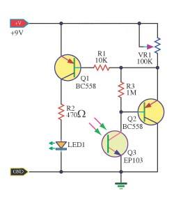
This is the simple Remote control tester circuit diagram. When the remote control is not working, first check the battery before, It may be loss.If it is good,so detect transmit infrared light device.However, because the human eye can not see infrared light,so can not know how good or bad.But the photo transistor can use to detect infrared light. 

This circuit so use this photo transistor is the light receiver from the remote control.If it is nice to have the bias current of the transistor BC558.It runs a current flows through the LED,so the LED bright.The remote control that works correctly. The variable resistor VR1 is used to adjust the sensitivity of the circuit.

 Remote control tester circuit diagram
 
 Remote control tester circuit diagram
Continue reading...

Simple 3 volt to 9 volt with LMC555 Circuit Diagram

| Labels: , , , , , , , , | 0 comments |
Simple 3 volt to 9 volt with LMC555 Circuit Diagram. This is a Build a 3 volt to 9 volt with LMC555 Circuit Diagram. This dc converter is built with the CMOS version of 555 timer. You can get 12V too if you change the zener diode to a 12V version.

3 volt to 9 volt with LMC555 Circuit Diagram


Build a 3 volt to 9 volt with LMC555 Circuit Diagram

Continue reading...

Simple Accurate Foot Switch Circuit Diagram

Tuesday, September 23, 2014 | Labels: , , , , , | 0 comments |
Certain industrial controls require accurate switching operations. For example, in case of a foot-switch for precise drilling work, even a small error in switching may cause considerable loss. This low-cost but accurate foot-operated switch can prevent that.

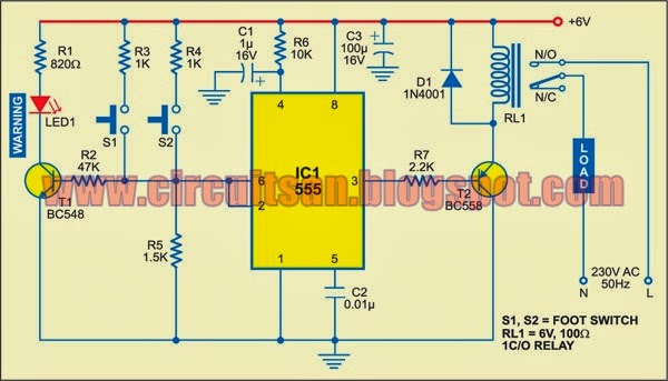
IC NE555 is wired in one-shot mode. Its output pin 3 goes high only when both switches S1 and S2 are pressed simultaneously. You can release any one of the switches without changing the output state. When you release both the switches, the output goes low.

Simple Accurate Foot-Switch Circuit Diagram

Simple Accurate Foot-Switch Circuit Diagram

The switches are placed under a foot paddle as shown in Fig. 2. LED1 is used as a warning indicator. If either S1 or S2 gets pressed erroneously, LED1 blinks to warn the operator. The operator can then withdraw his foot in case of a mistake or depress the other switch also to trigger the circuit. LED1 is to be mounted on the operator’s desk.

The circuit operation is simple. Resistors R2, R3 and R4 form a voltage divider. IC NE555 has two comparators, a flip-flop and power output section built into it. Pressing either S1 or S2 puts the input voltage between the upper comparator (2/3Vcc) and the lower comparator (1/3Vcc). Thus, it has no effect on the state of the internal flip-flop of IC NE555. Pressing the two switches simultaneously sets the flip-flop and the output of NE555 goes high. Transistor T2 energises relay RL1 for driving the load.


Releasing any of the switches brings the comparator voltage back to the initial level inside NE555 and it has no effect on the state of the flip-flop. Releasing both the switches brings the input level with respect to ground below the low trigger level, and thus it resets the output.

Use of the voltage divider results in stable operation over the entire permissible supply voltage range. The RC circuit at pin 4 provides power-on reset.

When only S1 is pressed, R3 (1 kilo-ohm) is less than R5 (1.5 kilo-ohms) and IC1 is not triggered. However, transistor T1 (BC548) gets forward biased and LED1 glows. When both S1 and S2 are pressed, the effective resistance between +Vcc and pin 2 of IC1 is about 500 ohms, which is less than R5 (1.5 kilo-ohms), and IC NE555 gets triggered.


Sourced By: EFY Author Name : Kaushik Hazarika
Continue reading...

Simple Cmos Motorcycle Alarm Circuit Diagram

Friday, September 19, 2014 | Labels: , , , , , | 0 comments |
This Simple Cmos Motorcycle Alarm Circuit Diagram features an intermittent siren output and automatic reset. It can be operated manually using a key-switch or a hidden switch; but it can also be wired to set itself automatically when you turn-off the ignition. By adding external relays you can immobilize the bike - flash the lights etc.

Cmos Motorcycle Alarm Schematic Diagram

Cmos Motorcycle Alarm Circuit Diagram

Notes
Any number of normally-open switches may be used. Fit "tilt" switches that close when the steering is moved or when the bike is lifted off its side-stand or pushed forward off its centre-stand. Use micro-switches to protect removable panels and the lids of panniers etc.

Once activated - the rate at which the siren switches on and off is controlled by R9 & C5. For example - increasing the value of C5 will slow it down - while reducing the value of R9 will make it faster.

While at least one switch remains closed the siren will sound. About thirty seconds after all of the switches have been opened, the alarm will reset. How long it takes to switch off depends on the characteristics of the actual components used. You can adjust the time to suit your requirements by changing the value of R6 and/or C4.

The circuit is designed to use an electronic Siren drawing 300 to 400mA. Its not usually a good idea to use the bikes own Horn because it can be easily located and disconnected. However, if you choose to use the Horn, remember that the alarm relay is too small to carry the necessary current. Connect the coil of a suitably rated relay to the "Siren" output. This can then be used to sound the Horn - flash the lights etc.

The circuit board and switches must be protected from the elements. Dampness or condensation will cause malfunction. Connect the 1-amp in-line fuse AS CLOSE AS POSSIBLE to your power source. This is VERY IMPORTANT. The fuse is there to protect the wiring - not the alarm. Exactly how the system is fitted will depend on the make of your particular machine - so Im unable to provide any further help or advice in this regard.

The quiescent (standby) current of the circuit is virtually zero - so there is no drain on the battery. If you want to operate the alarm manually use a key-switch or a hidden switch connected to the "off/set" terminals. For automatic operation connect a wire from the ignition circuit to the "ignit" terminal. Then every time you turn-off the ignition - the alarm will set itself. Remember that this wire from the ignition switch is not protected by your 1-amp inline fuse. So unless its run is very short - fit the wire with its own 1-amp fuse as close as possible to its source.

When you set the alarm - if one of the switches is closed - the siren will sound. This could cause annoyance late at night. A small modification will allow you to Monitor The State Of The Switches using LEDs. When the LEDs are all off - the switches are all open - and its safe to turn the alarm on.

Veroboard Layout

Cmos Motorcycle Alarm Circuit Diagram


Continue reading...

Simple DC to AC Inverter Circuit Diagram

| Labels: , , , , , , | 0 comments |
Simple DC to AC Inverter Circuit Diagram

Simple DC to AC Inverter

This DC to AC inverter circuit work based on unstable multi vibrator does. In this circuit, IC CD4047 is chosen as a heart of unstable multivibrator, because this IC type gives a complementary output that has opposite phase to another ( pin 10 and 11 as seen in Figure 1), and has 50 % duty cycle that satisfy to generate a pulse for inverter.
Continue reading...

Simple Frequency Comparator Circuit Diagram

| Labels: , , , , | 0 comments |
This is a digital circuit may arrive at your need, This circuit is a simple frequency comparator. The circuit Input 1 is used as a gating period, during which a single rising edge on input 2 will cause a logic 1 output-any other number, indicating non-identical frequencies causes a logic 0 output. ICla converts input 1 to a narrow pulse which initializes IC2 which forms a two-stage shift register clocked by input 2. 

 Best Frequency Comparator Circuit Diagram

Best Frequency Comparator Circuit Diagram
On the first edge of input 2 a logic 1 appears on the output of IC2b and for all subsequent inputs a logic 0 is present. At the end of the gating period this output is latched by IC3 forming the lock output.As this is only valid for one input period a monostable is added to the output to enable, for example, visual monitoring of the output. Either output from IC3 can be used depending on which state is most important. As connected the failure state is indicated. 
 
Sourced by : Circuitsstream
Continue reading...

Simple Photodiode Alarm Circuit Diagram

| Labels: , , , , | 0 comments |
Continue reading...

Simple Polyphonic DoorBell Circuit Diagram

| Labels: , , , , | 0 comments |
Here is an AC triggered Multitone, polyphonic doorbell. It gives eight melodious tunes for 2 minutes. On each press it will give a new tone which will continue till the melody is over. The circuit is too simple and battery operated It uses the popular melody generator IC UM3481.

The circuit uses the popular melody generator IC UM3481. It generates music tones like Jingle bell, Santa clause is coming, Silent night, Holy night, Joy to the world, Rudolph, Red nosed reindeer, Merry Christmas, O come, All Ye faithful, Hark and the herald angel sing.UM 3482 generates 12 music tones. Capacitor C1 and resistor R2 are the oscillation components. Pin1 can be triggered either by DC or AC. Here low voltage AC is applied to the trigger pin 1 through R1 and D1. The circuit works off two pen cells which last for more than one year

Polyphonic Door Bell Circuit Diagram

Polyphonic DoorBell Circuit Diagram


Caution:The circuit is connected to high volt AC. Do not touch any parts when it is powered to avoid lethal shock

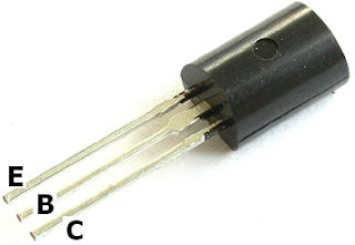
AC187 Pinout

AC187 Pinout

Continue reading...

Simple Multicell Charger Circuit Diagram

| Labels: , , , , | 0 comments |
Using this charger, you can safely charge up to two pieces of Ni-Cd cells or Ni-MH cells. The circuit is compact, inexpensive and easy-to-use.The 230V AC mains is down-converted to 12V AC (at 500 mA) by step-down transformer X1, converted into pulsating DC voltage by diodes D1 and D2, and fed to the battery charger terminals via current-limiting resistor R1 and silicon-controlled rectifier SCR1.

SCR1 is at the heart of the charger. Normally, it conducts due to the gate biasing voltage available through resistor R2 and diode D3, and the battery is in charging mode, which is indicated by LED1. Resistor R2 limits the charging current to a safe value. Charging current of this circuit is about 250 mA.

 Simple Multicell Charger Circuit Diagram


Simple Multicell Charger Circuit Diagram
When the battery reaches full charge, SCR2 conducts to pull down the gate of SCR1. This state is indicated by LED2. Now remove the cells from the charger. Normally, Ni-Cd cell with a rating of 500 mAH will take around 2.5 hours to reach full charge, while the charging time for Ni-MH cell with a rating of 1500 mAH will be around 7 hours. Charging time may vary depending on the settings of the charger and input supply line conditions. 

After construction, a minor adjustment is required for ensuring proper performance: Power on the circuit without cells and adjust VR1 such that LED2 lights up. Now measure voltage across the charger output terminals, which should be around 5V DC. Now insert the two cells into the holder and connect it to the charger output terminals for charging. LED1 instantly lights up to indicate the charging process. If LED1 glows dimly, readjust VR1 for proper glowing of LED1. Now the circuit is ready for use. Use of a small heat-sink is recommended for SCR1.


Sourced by: EFY Author: T.K. Hareendran
Continue reading...

Simple 25W Audio Power Amplifier Circuit

| Labels: , , , , , | 0 comments |
This audio power amplifier project is based on LM1875 amplifier module from National Semiconductor. It can deliver up to 30W of power using an 8 ohm load & dual 30V DC power supplies. It is designed to operate with maximum outside parts with current limit & thermal shutdown protection features . Other features include high gain, quick slew rate, wide power supply range, giant output voltage swing & high current capability.

Summary of the audio amply-fire features:

  • Low distortion: 0.015%, 1 kHz, 20 W
  • Wide power bandwidth: 70 kHz
  • Wide supply range 16V-60V
  • Up to 30 watts output power
  • Internal output protection diodes
  • Protection for AC & DC short circuits to ground
  • 94 dB ripple rejection
  • Plastic power package TO-220
25V Power Supply

The schematic below shows how the +25V DC & -25V DC are obtained. In order to provide power supply for two stereo amplifiers, a power transformer rating of 80VA with 240V/36V middle tapped secondary winding is used. The secondary output of the transformer is rectified by using 1N5401 diodes together with four electrolytic capacitors to smoother the ripple voltage. A fuse & a varistor are connected at the primary input to protect the circuit against power surge.


Audio Amplifier Module

The +25V & -25V DC power supply are connected to the audio amplifier module through a 2A fuse with the peripheral devices shown in the schematic below. The audio input signal to be amplified is coupled to pin one of LM1875 through the resistor R1 and electrolytic capacitor E5.

The output signal at pin four of LM1875 can be used to directly drive a 8 ohm loudspeaker. Resistor R6 and capacitor C5 prevent-the capacitance developed at the long speaker leads from driving the amplifier in to High Frequency Oscillation.

A heat-sink with a thermal resistance rating of one.4 Cecilius/Watt or better must be used or else the amplifier module will-be cut-off from operation due to the heat that will build up in the coursework of the operation of the amplifier. Take note that the heat sink tab on the IC module is internally connected to the -25V power supply hence it must be isolated from the heat sink by the use of an insulating washer. If this is not done, the negative rail will be shorted to ground.


Sourced By: Streampowers.blogspot.com
Continue reading...

Simple 3 volt to 9 volt with LMC555 Circuit Diagram

| Labels: , , , , , , , , | 0 comments |
Build a 3 volt to 9 volt with LMC555 Circuit Diagram. This is a Build a 3 volt to 9 volt with LMC555 Circuit Diagram. This dc converter is built with the CMOS version of 555 timer. You can get 12V too if you change the zener diode to a 12V version.

3 volt to 9 volt with LMC555 Circuit Diagram

Build a 3 volt to 9 volt with LMC555 Circuit Diagram

Continue reading...